Male Doctors, Female Cashiers: AI’s Job Bias This was originally posted on our Voronoi app. Download the app for free on iOS or Android and discover incredible data-driven charts from a variety of trusted sources. Key Takeaways AI-generated videos depict roughly 70%+ of high-paying roles, such as CEOs, software engineers, and financial analysts, as male.
AI Accelerator Testing Depends On DFT Innovations
Key Takeaways:
- I/O and lane repair capabilities are becoming critical to improving yield.
- System-level testing catches marginal defects and rare defects such as silent data corruption errors.
- Synopsys and TSMC developed a multi-die demo vehicle capable of full test, monitor, debug, and repair capability across the system’s lifecycle.
The proliferation of accelerators in AI chips is creating ripples throughout the test flow, requiring more test insertions, deeper analysis, and more monitoring throughout a device’s lifetime.
AI accelerators are custom hardware and software platforms built to speed parallel processing of neural networks, machine learning, and generative AI tasks. These multi-chiplet modules are enabling real-time processing for applications like autonomous vehicles, robotics, and adaptive testing of semiconductor chips. Design-for-test (DFT) techniques are rapidly improving to address the various challenges around rapidly transferring test content between dies, gaining better thermal control and heat removal from test beds, and developing new stress tests to exercise the new combinations of high power, temperature, and 24/7 workloads these accelerators require.

Fig. 1: Validating and testing die-to-die interfaces is critical in 2.5D and 3D packaging architectures. Source: Teradyne
As highlighted in the first installment of this two-article series, several aspects make AI module testing significantly more challenging than SoC testing:
- High current densities challenge thermal isolation and hotspot mitigation;
- Leading-node devices and interconnects like TSVs and hybrid bonds create new failure modes; and
- A lack of test access to die-to-die interfaces requires DFT innovation to fully test, debug, and repair faults (more on this later).
The magnitude of the problem is daunting. “Extreme architectural complexity and massive parallelism make DFT pattern generation and power management significantly more difficult for AI accelerators,” said Quoc Phan, technology enablement manager for 3D-IC DFT & Yield at Siemens EDA. “In addition, the extensive on-chip and external memory, with terabytes per second data transfer rates, creates significant difficulties for controllability and observability during manufacturing tests. And innovative DFT approaches are needed to reveal new failure modes and inter-die connectivity that traditional test methods struggle to address.”
As a result, chipmakers are growing more reliant on functional testing than in the past. “Because functional tests can analyze behavior across cores, chiplets, and memory (as opposed to structural test of isolated cores), they are one of the only ways to identify subtle defects and environmental marginalities,” wrote Advantest’s Ira Leventhal, vice president of U.S. applied research and technology, and Richard Lathrop, vice president of business development, in a recent article. [1] One approach to achieving the targeted test coverage and quality of multi-die assemblies is to shift as much functional test content as possible to the first test insertion, wafer probe.

Fig. 2: The yield pressures of multi-die integration are causing functional tests to shift left. Source: Advantest
This strategy is particularly important for multi-die assemblies. “Just like monolithic die testing, the goal in multi-die testing is to identify defects early,” said Faisal Goriawalla, principal product manager at Synopsys. “The difference is that the user needs to ensure that only known good parts are assembled to minimize debug and/or prevent costly field failure subsequently.”
That’s non-trivial, however. “The complexities within an advanced package have grown by a couple of orders of magnitude. These complexities are expected to grow even more as the number of package designs for each customer is unique,” said Vineet Pancholi, senior director of manufacturing test at Amkor. “With AI ASICs drawing 1,200 amps (soon 2,400 A levels), and because test systems must be capable of stressing devices to 2X the levels they would see in regular use, thermal management during testing is critical for these systems.”
That means the test systems must be equipped with exacting control of power resources during test, with precise regulation, fast clamping capability, and in-line monitoring of contact resistance. [1]
AI systems consist of massively replicated cores with a deep memory hierarchy. “If all these chiplets are the same, I’m not going to replicate vector data multiple times over multiple pins and just blast the same information to the part,” explained Daniel Simoncelli, business development manager for the P93k product line at Advantest. “I’ve got a streaming network architecture, SSN. But you want to run it faster, so we use PCIe. And the device is smart enough to distribute that content to all the different cores, so you don’t need to send the same data 10,000 times. Other features include the ability to do on-chip compare, instead of having the tester perform these checks, increasing testing efficiency.”
AI accelerator production testing priorities involve three main areas — the chiplet silicon blocks, the die-to-die interconnects, and the package-level connections for electrical, logic, and thermal performance,” said Amkor’s Pancholi. He noted that since AI logic blocks are scan-enabled, structural testing detects defects at the transistor level, which is no different than other advanced logic chips. “The EDA process flow outputs the automated test patterns. Fault modeling simulates traditional stuck-at and modern at-speed transition delays, and path delays are typically employed during chip probe at the wafer level and final test at the package level.”
Having more information about each die or chiplet in the package can help with matching chiplet performance. “Each die can come from a different supplier, and the packaging party can be even another business, so in bringing these together, I don’t think there is any magic solution,” said Shai Cohen, CEO of proteanTecs. “And there is the question of who is to blame when there is a problem because the cost of a failure is so much higher when you start assembling so many dies. But it is possible to get 10x better visibility into what’s going on inside each die, and also in between the dies on the interfaces using telemetry. And this can provide better visibility, for instance, during saw testing. You can avoid assembling defective dies onto a multi-die package. Also, there is an opportunity to select complementary dies from a performance, power, or yield standpoint so they work well with one another.”
One of the earliest applications of telemetry, or on-chip monitors, was to help detect silent data corruption (SDE). These rare workload-dependent errors only occur under certain environmental stress and workload conditions. In addition to helping detect these needle-in-a-haystack types of defect, telemetry can help with device aging, showing how much longer a given device is likely to operate, which improves preventive maintenance operations inside data centers.
But not all failures originate with the chiplets themselves. They can occur in the thousands, or even millions, of interconnections between chips and interposers. “Ensuring that TSVs in silicon interposers are functional is critical,” said Jeorge Hurtarte, senior director of product marketing in Teradyne’s Semiconductor Test Group. “We often focus on the die itself, but we can’t ignore these intermediate layers. The question is, ‘What can we do from a DFT perspective to ensure the integrity of these TSV structures?’ For example, could we embed some intelligence into the TSVs, essentially apply DFT principles to them? Adding intelligence could help ensure these structures are robust for both DC and AC testing. That could play a big role in improving both signal integrity and noise isolation.”
New failure modes
AI accelerator modules introduce several new and critical failure modes. “Signal integrity and crosstalk issues (like bridge faults and small delay defects) that traditional stuck-at models miss, are especially prevalent at high speeds and densities. And this noise can be worsened by signal interconnects in close proximity,” said Phan. “Additionally, mechanical and thermal contact defects in stacked dies can develop over time, requiring continuous monitoring and in-system testing. To mitigate these issues, I/O or lane repair capabilities are becoming crucial for improving yield by bypassing localized defects.”
Others concur on the origin of failures. “There are a variety of new failure modes [associated with AI modules],” said Scott Carroll, senior director of test business development at Amkor. “Most of these can be traced back to silicon defects or packaging defects or thermally-induced performance degradation.”
Power-aware ATPG can help with specific extrinsic failures. “Power is one of the key contributors to these failures. If power is not managed accurately during the ATPG patterns, it may lead to yield loss issues,” said Synopsys’ Goriawalla. ATPG patterns often have high toggle rates and could shoot the IR drop beyond the power budget, which is designed for functional mode of operation. That can cause false failures, and hence, yield loss.”
Die-to-die communications
There are two types of die-to-die interfaces. One is logic-to-logic, which is PHY-based, such as UCIe, or I/O-based, such as low-speed general-purpose I/O (GPIO). The second type is logic-to-memory (e.g., HBM PHY). Each has different DFT needs.
“These interfaces can be of many different types, governed by protocol standards with constraints in terms of partitioning (for example, mainband vs. sideband), running at different data rates, which may or may not have redundant lanes/schemes,” Goriawalla said. “This can make it challenging for DFT and SoC designers to effectively perform test, repair, pattern generation, silicon bring-up, debug, and diagnosis across and through all the types of interfaces.”
Because there is no access to traditional JTAG for in-system use, a commonly used on-chip interface such as Advanced Peripheral Bus (APB) must be deployed for test observability and control. And even with the existing IEEE standards (1149.1, 1500, 1687, 1838) and JEDEC standards for the interface IP, gaps remain.
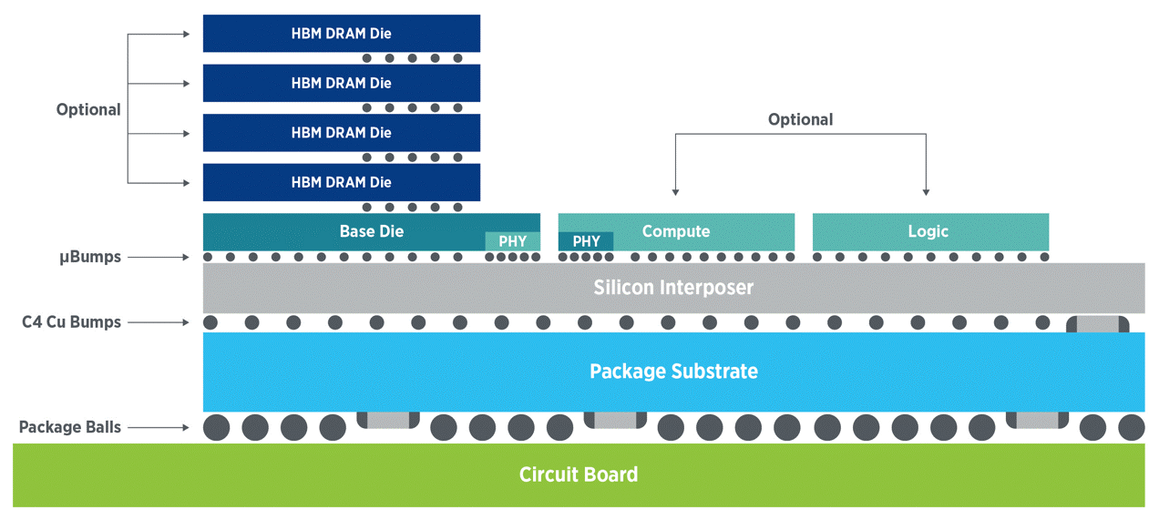
Synopsys and TSMC partnered in 2023 to develop a multi-die reference methodology based on CoWoS that could enable monitoring, testing, debugging, and repair across the silicon lifecycle, without loss of coverage or pattern inflation when targeting dies in a stack. One configuration used the UCIe interface to perform SLM monitoring, test, debug, and repair, while the second configuration used the GPIO interface consistent with the IEEE 1838 standard.

Fig. 3: Utilizing on-chip resources for UCIe PHY IP, this simplified block diagram of Synopsys-TSMC demo vehicle supports test, debug, and repair capabilities. Source: Synopsys
TSMC and Synopsys achieved comprehensive deployment across pre-bond and post-bond manufacturing stages, the in-field power-on stage, and mission-mode use case scenarios. This activity culminated in a successful two-chiplet and interposer tapeouts in late 2024. [2]
Siemens EDA’s Phan elaborated on techniques for verifying connectivity and functionality. “Boundary scan (1149.x) serves as a workhorse for testing interconnects at both the board and package levels,” he said. “It detects opens, shorts, and stuck-at faults at the board and package levels, including specialized support for high-speed differential interfaces (1149.6). Built-in self-test (BiST) for interfaces is crucial, with dedicated BiST for HBM data path verification (often utilizing HBM’s loopback mode and lane repair) and SerDes BiST (using loopback and PRBS) for high-speed serial links between xPUs. Finally, functional tests (at-speed) are essential for ultimate verification, involving large data transfers and performance benchmarks to ensure integrity and performance under real-world conditions.”
System-level testing
Unlike ATE and packaged device testing, system-level testing mimics actual operating conditions. By combining SLT of devices, peripherals, and software together in a realistic operating environment, companies can drive down escape rates to acceptable defective parts per million (DPPM) levels.
Marginal defects that only cause problems when multiple components are working together at high speeds, at certain temperatures, or when running particular software workloads, are particularly difficult to catch using ATE. Intel Foundry recently developed its own SLT modular platform to suss out rare defects such as SDEs. The system-level testing platform contains the same types of memory modules, storage devices, graphics cards, and network interfaces found in real systems.
“High-speed interface defects, which are particularly difficult to detect with traditional methods, become apparent when tested under realistic conditions with actual data traffic and electrical noise,” stated Vishwanath Natarajan, senior product development architect at Intel Foundry in a release. “SLT prevents issues such as USB device disconnections, audio glitches, and graphics performance problems that would otherwise frustrate users and damage product reputation.”
JohnDavid Lancaster, AI hardware research engineer at IBM Research, emphasized the importance of exceptionally high uptime and reliability in AI accelerators. “It’s important to exercise the full hardware stack under worst-case, high-stress workloads to ensure the AI system (chip, card) will not fail in the field. Therefore, we perform the worst-case LLM inference/hardware tests with full error, tensor result, and diagnostic checking. These tests adequately stress compute cores, memory interfaces, and power domains simultaneously.”
Each stage of the manufacturing process enables more of the final AI chip to be tested, starting at wafer test and culminating in the full chip being tested during SLT. Because many functions can only be tested at the end of the manufacturing process, SLT plays a critical role in ensuring consistency and reliability prior to field deployment.
The test suite in SLT is continuously refined through a feedback loop in which tests are run, failures are analyzed, workloads are refined, and screening criteria are then updated. Like many aspects of semiconductor testing, engineers encounter tradeoffs in test throughput versus test coverage. “Since manufacturing test time is limited, only a small subset of the most predictive and high-coverage tests can be run,” explained Lancaster. “Determining that minimal but sufficient set requires analyzing large amounts of failure and margin data from bring-up.”
By stressing parts with higher voltage and temperatures than they would normally encounter during actual use, burn-in mimics the aging process caused by defects and variability in the fab process. “Burn-in remains a crucial test insertion, especially for every new wafer fabrication process,” said Amkor’s Pancholi. “Weeding out infant mortality defects with early production volumes is indispensable. Burn-in at the wafer level is tough to accomplish and is still being done post-packaging.”
Conclusion
Since the advent of AI accelerators and multichip packaging, it’s become increasingly clear that testing across a chip’s lifecycle, from wafer probe to in-system testing, is needed to ensure 24/7 uptime of data centers. “It is essential that the AI accelerators incorporate design components to support in-field test and repair, so the tests can be enabled not only at manufacturing, but through the complete silicon lifecycle of the chips,” said Synopsys’ Goriawalla.
Design-for-test is also taking on increased importance, requiring built-in self-test of interfaces and dedicated BiST of HBM to provide loopback and lane repair, while SerDes BiST validates the high-speed links between processor chips. Power-aware ATPG helps prevent harmful power surges and false failures. Finally, system-level testing is playing a fundamental role in ensuring the functionality of AI modules prior to installation in data centers.
References
- Levinthal, I., Lathrop, R., “AI Chips Pose Demanding Test Challenges: An Exploration of New Methodologies,” in IEEE Electron Devices Magazine, vol. 3, no. 1, pp. 18-23, March 2025, doi: 10.1109/MED.2025.3540741.
- Zorian, Y., “Enabling Seamless Monitoring, Test, And Repair In Multi-Die Designs,” Semiconductor Engineering, March 10, 2026. https://semiengineering.com/enabling-seamless-monitoring-test-and-repair-in-multi-die-designs/
Related Articles
AI Accelerators Usher In New Era For IC Test
The number and variety of test interfaces, coupled with increased packaging complexity, are adding a slew of new challenges.
Optimizing DFT With AI And BIST
AI-driven automation, tighter design-test collaboration, and evolving BiST techniques are redefining DFT strategies.
Easing The Stress For Package-Level Burn-In
Employing more stress testing at the wafer level improves quality while reducing burn-in time and cost. So why isn’t it happening?
Related Posts