
Samsung Electronics is stepping up its AI transformation of the semiconductor business, recruiting specialists in deep learning and data engineering in quick succession. The company’s strategy is to build AI models tailored to semiconductor research and development alongside the data infrastructure AI systems need, raising development efficiency and productivity across design, process and manufacturing.
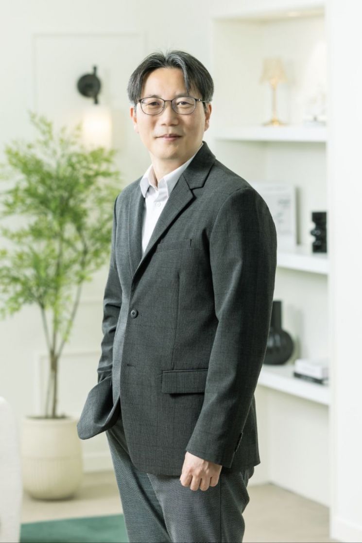
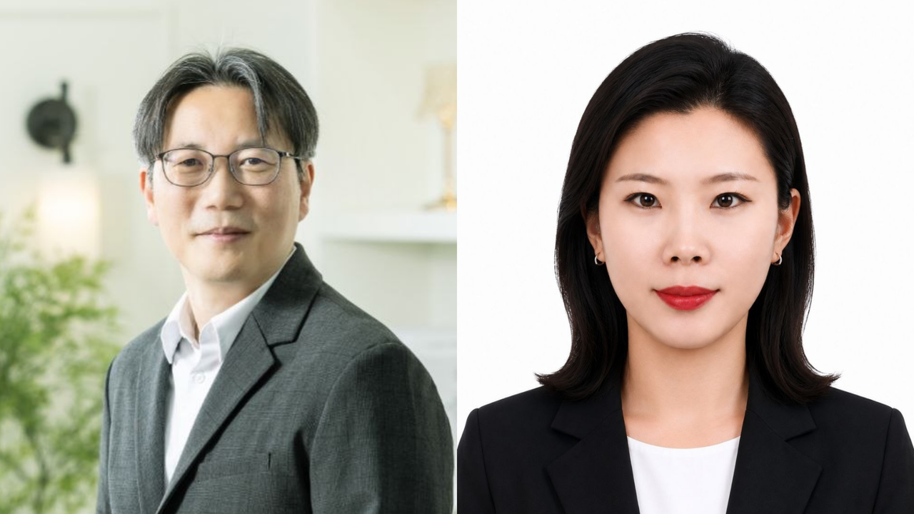
Samsung Electronics announced Friday that it has brought on Han Bo-hyung, a leading authority in deep learning and vision AI, as a fellow, and Han Tae-rin, a data engineering expert, as a senior vice president.
Han Bo-hyung will lead the development of AI models specialized for semiconductor R&D. He earned his bachelor’s and master’s degrees in computer science and engineering from Seoul National University before receiving a doctorate in computer science from the University of Maryland. He joined Pohang University of Science and Technology as an assistant professor of computer science and engineering in 2010 and served as a professor in the Department of Electrical and Computer Engineering at Seoul National University from 2018.
Vision AI refers to technology that enables computers to learn from large volumes of image and video data, then recognize objects and patterns and analyze their meaning. In the semiconductor industry, its applications are expanding across design, process and manufacturing, including wafer image analysis and defect detection.
Han Tae-rin will be responsible for building what the company calls “AI-ready data” — a data foundation that AI systems can immediately use for learning and analysis. Refining and structuring the vast amounts of data generated during semiconductor development and production into a form that AI can understand and use is essential to improving AI performance.
Han graduated from Seoul National University with a degree in mechanical and aerospace engineering and earned a master’s degree in mechanical engineering from the Massachusetts Institute of Technology. She worked at Meta as a senior engineering manager from 2016 and last year served as a senior developer at Persona in the United States.
The two hires reflect Samsung Electronics’ broader push to expand AI use across semiconductor design, process and manufacturing.
Samsung Electronics’ Device Solutions division outlined an “agentic AI”-based semiconductor engineering strategy at Nvidia GTC 2026 in the United States in March, describing how AI would connect the entire semiconductor value chain from design and engineering through to manufacturing. The division said it would use agentic AI and digital twin technology to ensure stable quality management.
Samsung Electronics plans to continue expanding AI adoption across core semiconductor operations including design, process and manufacturing. Alongside this, the company intends to keep recruiting top talent in AI and data and to spread their expertise throughout the organization to strengthen its AI capabilities company-wide.